
基于树莓派实现的智能小车论文
树莓派3是一款基于ARM的微型电脑主板,具备所有PC的基本功能,Python作为主要编程语言,系统基于Linux或者Windows 10 IoT,有良好的易用性和多功能性。这里介绍的是如何用树莓派3来实现太原理工大学的毕业设计,该设计是树莓派结合多个传感器的智能小车的发明,是未来多个行业的发展方向,它可以按照程序预先设定好的模式在一个符合设定程序的环境里自动的运作,不需要人为的管理,可应用于科学勘
收藏关注不迷路
基于树莓派实现的智能小车论文
一、摘 要
树莓派3是一款基于ARM的微型电脑主板,具备所有PC的基本功能,Python作为主要编程语言,系统基于Linux或者Windows 10 IoT,有良好的易用性和多功能性。这里介绍的是如何用树莓派3来实现太原理工大学的毕业设计,该设计是树莓派结合多个传感器的智能小车的发明,是未来多个行业的发展方向,它可以按照程序预先设定好的模式在一个符合设定程序的环境里自动的运作,不需要人为的管理,可应用于科学勘探、科研、军事等的用途。
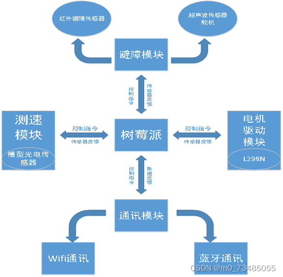
本系统为实现设计题目的要求,采用了树莓派3为控制核心,接收并处理传感器消息;利用超声波传感器与舵机相结合或使用红外线传感器检测道路上的障碍,控制智能小车的自动避障,并且可以自动记录小车运行速度;利用ssh键盘控制或spp手机app蓝牙遥控或通过手机app遥控。
整个小车系统的电路结构简单(采用树莓派的GPIO为核心省去单片机最小系统的设计),可靠性能高(树莓派的优越性)。实验测试结果满足预期要求,本文将着重介绍了该小车系统的硬件设计方法及软件实现方式以及测试结果分析。
采用的技术主要有:
(1)通过编程来控制小车运行;
(2)传感器的有效应用;
(3)ssh通讯、蓝牙spp通讯、wifi通讯.
Intelligent car based on Raspberry Pi
Abstract
Raspberry Pi 3 is a ARM based microcomputer board with all of the basic functions of PC, Python as a major programming language, the system is based on Linux or Windows 10 IoT, has good ease of use and functionality. Here is how to use PI 3 to implement the graduation design of Taiyuan University of Technology, the design is combined with raspberry pie intelligent car multiple sensors of the invention, is the future development direction of many industries, it can be programmed to preset mode in a line with the automatic operation of the set program environment, not the need of human management, application of scientific exploration, scientific research, military etc…
This system in order to achieve the design requirements of the subject, using the raspberry pi 3 as control core, receiving and processing of sensor information; using ultrasonic sensors and actuator combination or use infrared sensors to detect obstacles on the road, automatic obstacle avoidance of intelligent vehicle control, and can automatically record the running speed of car; use the SSH keyboard or spp mobile phone app mobile phone through Bluetooth remote control or remote control app.
The circuit structure of the whole car system is simple (using raspberry pie GPIO as the core, eliminating the minimum system design of single chip microcomputer), and the reliability is high (the superiority of raspberry pie). The experimental results meet the expected requirements. This paper will focus on the hardware design method and software implementation of the car system and test results analysis.
The main technologies used are:
(1)control the operation of the car by programming;
(2)Efficient application of the sensor;
(3)SSH communication, Bluetooth spp communication, WiFi communication
Key words: Raspberry Pi 3 Ultrasonic Infra-red smart car
二、目 录
目录
摘 要 I
Abstract II
- 前 言 1
1.1 树莓派是什么? 1
1.2 树莓派启动方式及支持的系统 2
1.3 镜像烧写 2
1.4 开发板供电 3
1.5 GPIO模块 3 - 方案设计与论证 4
2.1 直流调速系统 4
2.2 检测系统 5
2.2.1 行车距离检测 5
2.2.2 行车速度检测 5
2.3 通讯模块 7
2.3.1 蓝牙通讯 7
2.2.2 WIFI通讯 8
2.3 系统原理图 8 - 硬件设计 9
3.1 树莓派3硬件结构 9
3.1.1硬件配置 9
3.1.2 系统安装及环境配置 10
3.1.2.1 系统烧写 10
3.1.2.2 系统环境配置 10
3.1.2.3 软件环境配置 10
3.2 车轮电路设计 12
3.2.1 L298N 12
(1)模块工作原理 12
(2)控制方式 12
(3)管脚介绍 12
3.2.2 直流电机 13
3.3 测速模块设计 13
3.4 红外避障设计 13
3.4.1 YL-70传感器 13
(1)模块工作原理 13
(2)控制方式 13
(3)管脚介绍 14
3.5 超声波避障设计 14
3.5.1 超声波模块HC-SR04 14
(1)模块工作原理 14
(2)管脚介绍 15
3.5.2 舵机SG90 15
(1)模块工作原理 15
(2)管脚介绍 15
(3)舵机的控制 15 - 软件设计 16
4.1环境准备 16
4.1.1 环境安装 16
4.1.2 开发语言(GPIO编程) 19
(1)python GPIO 19
(2)wiringPi 19
(3)BCM2835 C Library 20
(4)语言选择 21
4.1.3软件安装 21
(1)redis 21
(2)Python操作Redis 22
4.2程序设计 23
4.2.1 信息采集子程序设计 23
4.2.2 信息处理分析子程序设计(主程序) 23
4.2.3 运动控制子程序设计 23
4.2.4 工作状态子程序技术 24
4.2.5 通讯程序技术(主程序) 24 - 测试数据、测试结果分析及结论 25
- 致 谢 25
- 参 考 文 献 26
附录A 程序清单 27
附录程序1 27
附录程序2 27
附录程序3 28
附录程序4 28
附录程序5 31
附录程序6 32
附录程序7 33
附录程序8 34
附录B 硬件原理图 35
图1 35
图2 36
图3 36
图4 37
外文翻译 38
英文原文 38
中文翻译 46
三、前 言
1.1 研究背景
随着汽车工业和机器人的迅速发展,关于机器人的研究也就越来越受人关注。全国电子大赛和省内电子大赛以及高校校内的竞赛几乎每次都有智能小车这方面的题目,全国各高校对该题目的研究都很重视。可见其研究意义很大很有价值。
本设计就是在这样的背景下提出的,本题目是结合科研项目和未来发展趋势而确定的设计类课题。设计的智能小车应该能够实时显示速度,具有自动避障功能,可程控行驶方向。
根据题目的要求,确定如下方案:在现有的小车亚克力框架基础上,加装光电传感器(红外传感器、光电对射传感器)、超声波传感器及舵机,从而实现对智能小车的位置、速度、运行状况的实时控制和实时测量,并将测量数据(传感器数据即GPIO口电位变化)传送至树莓派进行处理,然后由树莓派根据所检测的各种数据实现对智能小车的智能控制或由树莓派将小车运行状态或运行数据传送至手机app来进行对小车的手动控制。
这种方案能实现对智能小车的运动状态进行实时控制,控制方法灵活且可靠,精度高,可以满足系统的各项要求。以树莓派3为控制核心,利用超声波传感器结合舵机或者单独利用红外灵活检测道路上的障碍,控制智能小车的自动避障,行驶,并可以自动记录运行速度。
1.1 树莓派是什么?
Raspberry Pi(中文名为“树莓派”,简写为 RPi,或者 RasPi/RPi)是为学生计算机编程教育而设计,只有信用卡大小的卡片式电脑,其系统基于 Linux。
树莓派由注册于英国的慈善组织 “Raspberry Pi 基金会”开发,Eben·Upton /埃·厄普顿为项目带头人。2012 年 3 月,英国剑桥大学埃本·阿普顿(Eben Epton)正式发售世界上最小的台式机,又称卡片式电脑,外形只有信用卡大小,却具有电脑的所有基本功能,这就是Raspberry Pi 电脑板,中文译名"树莓派"!这一基金会以提升学校计算机科学及相关学科的教育,让计算机变得有趣为宗旨。基金会期望这一款电脑无论是在发展中国家还是在发达国家,会有更多的其它应用不断被开发出来,并应用到更多领域。
就像其他任何一台运行Linux 系统的台式计算机或者便携式计算机那样,利用Raspberry Pi 可以做很多事情。当然,也难免有一点点不同。普通的计算机主板都是依靠硬盘来存储数据,但是Raspberry Pi 来说使用SD 卡作为“硬盘”,你也可以外接USB 硬盘。利用Raspberry Pi 可以编辑Office 文档、浏览网页、玩游戏—即使玩需要强大的图形加速器支持的游戏也没有问题
Raspberry Pi 的低价意味着其用途更加广泛,将其打造成卓越的多媒体中心也是一个不错的选择。利用Raspberry Pi 可以播放视频,甚至可以通过电视机的USB 接口供电。
一句话:树莓派是一个卡片大小的开发板,上面可以运行 Linux 系统,我们可以用它开发我想要的设备硬件方面
Broadcom为Raspberry Pi 3带来了全新的BCM2837 SoC,它保留了与MCB2835和BCM2836相同的基础架构,所以大量依赖于特定硬件细节的项目仍可继续工作
网络方面,Raspberry Pi 3还直接板载了802.11n Wi-Fi和蓝牙4.1支持
本设计就采用了比较先进的64位四核ARM Cortex 1.2GHz处理器为控制核心。使这款小型设备更为实用的并不是它更快的处理器,而是它的网络支持,例如可穿戴的血压监控器将与房间中的恒温器与暖气阀门想沟通,又或者能联系当地的医生寻求建议。而在工作场所中,每个设备将具备联网能力,传感器也将能处理数据。最新的树莓派的到来使这一切距离现实更近一步该设计具有实际意义,可以应用于物联网项目的硬件平台选择。所以本设计与实际相结合,现实意义很强。
1.2 树莓派启动方式及支持的系统
树莓派开发板没有配置板载 FLASH,因为它支持 SD 卡启动,所有我们需要下载相应镜像,并将其烧写在 SD 上,启动系统即可 (这个镜像里包含了我们通常所说的 bootloader、kernel、文件系统) 树莓派由于其开源特性,支持非常多的系统类型(指的文件系统):Raspbian、Arch Linux ARM、Debian Squeeze、Firefox OS、Gentoo Linux Google Chrome OS、Raspberry Pi Fedora Remix、Slackware ARM QtonPi、Slackware ARM、WebOS、RISC OS、FreeBSD NetBSD、Android 4.0(Ice Cream Sandwich)
1.3 镜像烧写
准备工作
- 一张 16g的 Class 10 高速卡SD 卡及读卡器,卡的速度直接影响树莓派的运行速度,选用大内存否则后续开发会使用经常不够用
- WinXP 和 Win7 下安装镜像的工具:Win32DiskImager.zip 同样在上一步的网址下载
- 上一步下载好的镜像
安装 - 解压下载的系统压缩文件,得到 img 镜像文件
- 将 SD 使用卡托或者读卡器后,连上电脑
- 解压并运行 win32diskimager 工具
压缩界面
- 在软件中选择 img 文件,“Device”下选择 SD 的盘符,然后选择“Write”然后就开始安装系统了,根据你的 SD 速度,安装过程有快有慢。
- 安装结束后会弹出完成对话框,说明安装就完成了,如果不成功,请关闭防火墙一类的软件,重新插入 SD 进行安装,请注意安装完,win 系统下看到 SD 只有 50MB 了,这是正常现象,因为 linux 下的分区 win 下是看不到的,通常只显示50m的boot分区
1.4 开发板供电
树莓派开发板有两种供电方式:
使用 micro usb 供电:所有 android 手机的充电线都可以给他供电
外接电源直接供电:B 型(B+型)GPIO 左上角的 2、4 管角为电源正极,6 管角为地
1 、2针脚5v, 3针脚GND
1.5 GPIO模块
该程序包提供了一个在 Raspberry Pi 中控制 GPIO 的类。
注意,该模块不适合应用到追求实时性或计数周期的应用中。这是由于您无法预测 Ptyhon 何时繁忙,以及资源回收的时间。而且它是运行在基于 Linux 核心的系统中,也不合适用于实时应用 - 原因在于其它进程可能获得更高的 CPU 优先级
二、 方案设计与论证
根据题目的要求,确定如下方案:在现有的小车框架基础上,加装光电、红外线、超声波传感器及舵机,实现对智能小车的速度、位置、运行状况的实时测量,并将测量数据传送至树莓派进行处理,然后由树莓派根据所检测的各种数据实现对智能小车的智能控制或由树莓派传送至手机app进行手动控制。
2.1 直流调速系统
方案一:采用数控电位器调整电动机的分压,从而达到调速的目的。但是数控电阻的元器件价格比较昂贵,不实用。更主要的问题在于一般电动机的电阻很小,但电流很大;分压会降低效率,而且实现也很困难。
方案二:采用继电器对电动机的开或关进行控制,通过开关的切换对小车的速度进行调整,这个方案的优点是电路较为简单,缺点是继电器的响应时间慢、机械结构易损坏、寿命较短、可靠性不高。
方案三:采用具有防止单边短路保护设计的H型PWM电路。脉宽调制(PWM)是指用微处理器的数字输出来对模拟电路进行控制,是一种对模拟信号电平进行数字编码的方法。由树莓派直接产生PWM信号,使之工作在占空比可调的开关状态,控制H型桥式PWM电机驱动电路,精确调整电动机转速。这种电路由于工作在管子的饱和截止模式下,效率非常高,H 型电路保证了可以简单地实现转速和方向的控制;电子开关的速度很快稳定性也极强.是一种广泛采用的PWM调速技术。且PWM调速系统有下列优点:
(1)由于PWM调速系统的开关频率较高,仅靠电枢电感的滤波作用就可以获得脉动很小的直流电流,电枢电流容易连续,系统的低速运行平稳,调速范围较宽,可达1:10000左右。
(2)同样由于开关频率高,若与快速响应的电机相配合,系统可以获得很宽的频带,因此快速响应性能好,动态抗扰能力强。
(3)由于电力电子器件只工作在开关状态,主电路损耗较小,装置效率较高。
根据以上综合比较,以及本设计中受控电机的容量和直流电机调速的发展方向,且在树莓派上,可以通过对GPIO的编程来实现PWM
基于以上讨论本设计采用了双H桥电机驱动L298N对直流电机驱动和调速。
2.2 检测系统
检测系统主要实现利用各种传感器对智能小车的避障、位置、行车状态进行测量。
2.2.1 行车距离检测
方案一:超声波测距传感器
超声波对固体或液体的穿透本领很大且超声波碰到物体会产生显著反射形成反射成回波,因此计算并处理超声波发出到接收回波的时间差即可得到距离。
方案二:红外线测距传感器
利用红外信号遇到障碍物的距离不同同时反射的强度也不同的原理,进行障碍物远近的检测,通过接收管接收发射管发射的特定频率的红外线所遇到障碍物体反射回来的红外信号,经处理后即可利用识别红外返回信号识别周围环境的变化
方案三:激光测距传感器
由激光二极管所发出的激光脉冲经目标向各方向反射后被光学系统检测,记录并处理计算出光脉冲发出到接收的时间差即可得到距离。
方案选择理由
虽然激光测距传感器测量精度高量程大但由于光速过快无法测量距离过近的物体且对光线较敏感无法在室外正常工作,故不选择方案三。
利用超声波进行检测往往比较迅速和方便,并且计算简单,而且易于做到实时控制,在测量精度方面能达到该课题的实用的要求,因此使用在智能小车的躲避障碍的应用。
为弥补超声波测距反应慢、且由于声波相互干扰不能同时检测的特点,故同时加配了红外传感器,用于补充,由于有同步输入端,可多个传感器同步测量。同时由于红外对和白色的反射不同也可以用于循迹
方案最终结果
基于以上讨论本设计采用超声波测距避障,并辅以红外避障
2.2.2 行车速度检测
方案一:电磁式-霍尔传感器
利用霍尔效应原理,在轴上安装一个小磁铁,轴旋转的时候,当磁铁经过霍尔器件时,器件会产生一个低电平的脉冲,而没有磁铁经过时,则是高电平。这样的话只要数低电平的数目就知道转了几圈。如果事先知道轮子的半径,就可以计算出周长,进而根据旋转圈数计算出里程。如果同时有时间计量,就知道了速度。
方案二:光电式-光电传感器
利用光电对射原理。也就是在轴上套一个光栅,也就是一个像自行车轮子一样的圈(当然很小),上面有很多辐条。然后左右装一个光电(红外)发射、接收管。如果发射后的信号被接收,出高电平,如果被辐条遮挡就产生一个低电平。事先辐条的数量是知道的,比如100条,根据测量到的低电平数量,然后除以100,就是转过的圈数。后面的测速跟前面电磁式是一样的。
光电传感器方案:
⑴槽型光电传感器
把一个光发射器和一个接收器面对面地装在一个槽的两侧的是槽形光电。发光器能发出红外光或可见光,在无阻情况下光接收器能收到光。但当被检测物体从槽中通过时,光被遮挡,光电开关便动作。输出一个开关控制信号,切断或接通负载电流,从而完成一次控制动作。槽形开关的检测距离因为受整体结构的限制一般只有几厘米。
⑵对射型光电传感器
若把发光器和收光器分离开,就可使检测距离加大。由一个发光器和一个收光器组成的光电开关就称为对射分离式光电开关,简称对射式光电开关。它的检测距离可达几米乃至几十米。使用时把发光器和收光器分别装在检测物通过路径的两侧,检测物通过时阻挡光路,收光器就动作输出一个开关控制信号。
⑶反光板型光电开关
把发光器和收光器装入同一个装置内,在它的前方装一块反光板,利用反射原理完成光电控制作用的称为反光板反射式(或反射镜反射式)光电开关。正常情况下,发光器发出的光被反光板反射回来被收光器收到;一旦光路被检测物挡住,收光器收不到光时,光电开关就动作,输出一个开关控制信号。
⑷扩散反射型光电开关
它的检测头里也装有一个发光器和一个收光器,但前方没有反光板。正常情况下发光器发出的光收光器是找不到的。当检测物通过时挡住了光,并把光部分反射回来,收光器就收到光信号,输出一个开关信号。
方案选择理由
一般来说,光电式的精度要更高一些,而且由于距离的限制本方案选用槽型光电传感器
方案最终结果
选择槽型光电传感器并辅以光电编码盘对小车速度进行检测
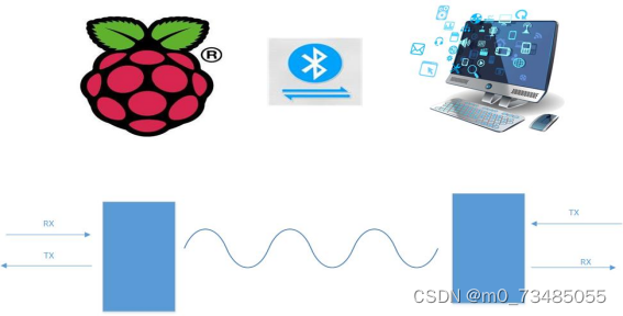
2.3 通讯模块
2.3.1 蓝牙通讯
蓝牙技术
蓝牙是一个使用广泛的无线通信协议,这两年又随着物联网概念进一步推广。根据细节上的差别,蓝牙通信又细分为两种:经典蓝牙和低功耗蓝牙。早期的蓝牙通信方式称为经典蓝牙(classic bluetooth)。经典蓝牙中的数据传输协议是串行仿真协议RFCOMM。RFCOMM仿真了常见的串口连接。数据从一端输入,从另一端取出。经典蓝牙的开发非常简单。基于串口开发的有线键鼠程序,就可以直接用于RFCOMM连接的无线键鼠。此外,经典蓝牙可以快速传输数据。因此,诺基亚N95这样的早期智能手机,也用RFCOMM来互传图片和文件。
这里介绍蓝牙协议,并用树莓派来实践。树莓派3中内置了蓝牙模块。树莓派通过UART接口和该模块通信。
安卓平台提供对蓝牙的通讯栈的支持,允许设备和其他的设备进行无线传输数据。应用程序层通过安卓API来调用蓝牙的相关功能,这些API使程序无线连接到蓝牙设备,并拥有P2P或者多端无线连接的特性
树莓派蓝牙通讯
需要环境
树莓派上使用蓝牙需要下载BlueZ,BlueZ是Linux官方的蓝牙协议栈,且树莓派的蓝牙需设置在兼容模式下启动
在本次设计中需要树莓派的原生蓝牙与手机进行通讯,需要协议spp(Serial Port Profile)来对双方进行规定。关于SPP,它是一个传输协议子集,它规定了在两个对等设备之间建立RFCOMM通信所需要的基本操作。串口应用基于通用访问应用GAP和服务发现应用SDAP应用模型之上,又是其他许多应用框架的基础。SPP可以直接映射到RFCOMM协议中,当两个设备间需要通过RFCOMM仿真的串口进行通信时,SPP对其中必备的服务和过程做出详细的规定。
在本次设计中开发语言使用Python,对于Python直接调用蓝牙串口进行通信在Github上找到了一个pybluez的库,提供了基于套接字的蓝牙串口通信接口。
2.2.2 WIFI通讯
由于树莓派的开启执行没有实体按钮,需要外接显示器来进行操作,在没有外接显示器的情况下可以通过路由器创建的WiFi将树莓派与电脑构建到同一局域网内,这样通过远程登陆协议ssh远程登陆对树莓派进行命令行或者vnc远程登录进行图形化界面操作
SSH 是较可靠,专为远程登录会话和其他网络服务提供安全性的协议。利用 SSH 协议可以有效防止远程管理过程中的信息泄露问题
在本次设计中需要树莓派原生WiFi与电脑进行通讯故使用Xshell作为远程登陆的命令行操作软件,FileZilla Client作为文件或代码在Windows和Linux平台间的文件传输软件,VNC-Viewer作为远程登陆的图形化操作软件
2.3 系统原理图
三、 硬件设计
3.1 树莓派3硬件结构
3.1.1硬件配置
![型号
3代B型
SOC[4] Broadcom BCM2837
CPU ARM Cortex-A53 1.2GHz 64-bit quad-core ARMv8 CPU
GPU Broadcom VideoCrore IV,OpenGL ES 2.0,1080p 30 h.264/MPEG-4
AVC高清解码器
内存 1GB (LPDDR2)
网络接口 10/100以太网接口
802.11n Wireless LAN
Bluetooth 4.1
Bluetooth Low Energy (BLE)
外设 17个GPIO及HAT规格铺设
操作系统 Debian GNU/Linux 、Fedora、Arch Linux 、RISC OS, Windows10 IoT[6]](https://img-blog.csdnimg.cn/ce2bbe38c3f3476f924cc8c073da13bf.png)
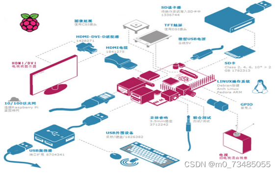
树莓派整体结构图
3.1.2 系统安装及环境配置
3.1.2.1 系统烧写
第一步:先下载系统
Raspbian “Jessie”是Debian8.0在ARM的编译版,加上针对树莓派深度定制的硬件驱动与软件程序。官方推荐系统。
第二步:烧写下载的系统
利用镜像的安装工具‘Win32DiskImager’将下载好的系统镜像烧写到内存卡中
第三步,修改 config.txt 配置文件
不修改配置文件会出现无法启动或显 示器不亮(黑屏)、无信号、分辨率太大,画面显示不全,等等一些问题
由于使用的最新版系统中ssh默认禁止,按官方指导在root分区下创建ssh文件即可
3.1.2.2 系统环境配置
利用路由器构成的局域网并将树莓派与笔记本至于该局域网下,笔记本采用无线连接,树莓派首次采用网线连接,通过路由器后台获取树莓派由路由器DHCP所产生的IP。
在Windows下,利用Xshell软件利用已获知的树莓派ip进行ssh即远程登陆树莓派
更换系统源,由于raspberry官方系统源下载更新过慢,更换至国内阿里源后更新系统
安装图形化远程连接软件vnc并配置
3.1.2.3 软件环境配置
一、GPIO开发
【python GPIO】
【开发语言】——python
【简单介绍】——该库更确切的名称为raspberry-gpio-python,树莓派官方资料中推荐且容易上手。python GPIO是一个小型的python库,可以帮助用户完成raspberry相关IO口操作。但是python GPIO库还没有支持SPI、I2C或者1-wire等总线接口。除了python GPIO之外,还有众多的python扩展库(例如webiopi),毫无疑问的说python非常适合树莓派,树莓派也非常适合python。
【wiringPi】
【开发语言】——C语言
【简单介绍】——wiringPi适合那些具有C语言基础,在接触树莓派之前已经接触过单片机或者嵌入式开发的人群。wiringPi的API函数和arduino非常相似,这也使得它广受欢迎。作者给出了大量的说明和示例代码,这些示例代码也包括UART设备,I2C设备和SPI设备等,毫无疑问地说wiringPi功能非常强大。

【BCM2835 C Library】
【开发语言】——C语言
【简单介绍】BCM2835 C Library可以理解为使用C语言实现的相关底层驱动,它给我的感觉更像STM32的库函数,BCM2835 C Library的驱动库包括GPIO、SPI和UART等,可以通过学习BCM2835 C Library熟悉BCM2835相关的寄存器操作。如果有机会开发树莓派上的linux驱动,或自主开发python或PHP扩展驱动,可以从BCM2835 C Library找到不少的“灵感”。
二、开发语言环境安装
Python2.7 与python 3raspberry系统内置,故只需更新系统即可
安装编辑环境VIM
蓝牙环境安装bluez,由于树莓派源中不是最新版,需手动下载安装
安装pybluez库,pybluez库会在使用pip安装时自动编译相关的蓝牙库,所以需要在安装pybluez之前先把蓝牙开发环境配置好(pybluez库的接口和Python中对于TCP的socket模块接口类似)
三、开发软件
Windows下使用:
Xshell File进行远程命令行执行
VNCserver进行远程图形化操作
Zilla Client进行代码传输文件传输
利用串口助手对手机与树莓派蓝牙通讯检测
Raspberry系统下:
利用Xgcom软件对手机与树莓派蓝牙通讯检测
VNCserver进行对图形化远程操作响应
VIM对代码修改编辑
Android系统(手机):
下载蓝牙串口助手对手机与树莓派蓝牙通讯检测
JuiceSSH进行远程命令行执行
VNC Viewer进行远程图形化操作
蓝牙串口助手下配置如下:
3.2 车轮电路设计
3.2.1 L298N
(1)模块工作原理
L298N是专用驱动集成电路,属于H桥集成电路,与L293D的差别是其输出电流增大,功率增强。其输出电流为2A,最高电流4A,最高工作电压50V,可以驱动感性负载,如大功率直流电机,(二相、三相、四相)步进电机,伺服电机,电磁阀等,特别是其输入端可以与单片机直接相联,从而很方便地受单片机控制。当驱动直流电机时,可以直接控制两路电机,并可以实现电机正转与反转,实现此功能只需改变输入端的逻辑电平。
本模块具有体积小,控制方便的特点。采用此模块可以应对需要大功率直流电机的题目。
(2)控制方式
L298N芯片,是一款双桥驱动芯片,支持两个直流电机和一个步进电机的驱动
驱动直流电机规则如下图
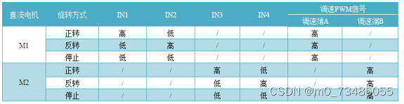
L298N驱动直流电机规则
电路图见附录B 图1
(3)管脚介绍
接线端接口:
VCC:电源输入正极
GND:电源输入负极
OUT1、OUT2:第一路桥输出
OUT3、OUT4:第二路桥输出
排针接口:
GND:电源负极,作为板子公共端
+5V:内部5V稳压芯片输出
IN1、IN2:第一路桥输入
IN3、IN4:第二路桥输入
ENA:第一路桥的输入使能开关,对于直流电机这里可接PWM调制控制速度,对于步进电机这里则接高电平使能。
ENB:第二路桥的输入使能开关,与ENA相同
3.2.2 直流电机
工作参数
工作电压 DC 3V DC 5V DC 6V
工作电流 100ma 100ma 120ma
减速箱减速比 48/1
空载(加轮子) 100转/分 190转/分 240转/分
空 载 速 度 20米/分 39米/分 48米/分
噪声 <65db
3.3 测速模块设计## 标题模块工作原理
1.模块槽中无遮挡时,接收管导通,模块 OUT 输出低电平,遮挡时,OUT 输出高电平;
2、OUT 输出接口可以与树莓派GPIO 口直接相连,检测传感器是否有遮档,如用电机码盘则可检测电机的转速
原理图见附录B 图2 光电测速结构图见附录B 图4
管脚介绍
VCC 接电源正极 3.3-5V
GND 接电源负极
OUT TTL 开关信号输出
3.4 红外避障设计
3.4.1 YL-70传感器
(1)模块工作原理
此模块是为智能小车、机器人等自动化机械装置提供一种多用途的红外线探测系统的解决方案。该传感器模块对环境光线适应能力强,其具有一对红外线发射与接收管,发射管发射出一定频率的红外线,当检测方向遇到障碍物(反射面) 时,红外线反射回来被接收管接收,经过比较器电路处理之后,同时信号输出接 口输出数字信号(一个低电平信号),可通过电位器旋钮调节检测距离,有效距 离范围 2~60cm,工作电压为 3.3V-5V。该传感器的探测距离可以通过电位器调节、具有干扰小、便于装配、使用方便等特点,可以广泛应用于机器人避障、避障小车、流水线计数及黑白线循迹等众多场合。
(2)控制方式
1 当模块检测到前方障碍物信号时,电路板上红色指示灯点亮,同时 OUT 端口持续输出低电平信号,该模块检测距离 2~60cm,检测角度35°,检测距离可以通过电位器进行调节,顺时针调电位器,检测距离增加;逆时针调电位器,检测距离减少。 2、传感器属于红外线反射探测,因此目标的反射率和形状是探测距离的关键。其中黑色探测距离最小,白色最大;小面积物体距离小,大面积距离大。
3、传感器模块输出端口 OUT 可直接与单片机 IO 口连接即可,也可以直接驱动一 个 5V 继电器模块或者蜂鸣器模块;连接方式:VCC-VCC;GND-GND;OUT-IO
4、比较器采用 LM339,工作稳定;
5、可采用 3.3V-5V 直流电源对模块进行供电。当电源接通时,绿色电源指示灯点亮
原理图见附录B 图3
(3)管脚介绍
VCC 接电源正极 3.3-5V
GND 接电源负极
Int1-4 开关信号输出
3.5 超声波避障设计
3.5.1 超声波模块HC-SR04
(1)模块工作原理
(1)采用 IO 触发测距,给至少 10us 的高电平信号;
(2)模块自动发送 8 个 40khz 的方波,自动检测是否有信号返回;
(3)有信号返回,通过 IO 输出一高电平,高电平持续的时间就是
(4)超声波从发射到返回的时间.测试距离=(高电平时间*声速(340M/S))/2;
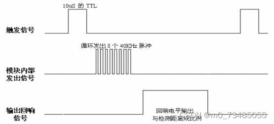
超声波时序图
以上时序图表明你只需要提供一10u以上脉冲触发信号,该模块内部将发8个 40kHz周期电平并检测回波。一旦检测到有回波信号则输出回响信号。 回响信号的脉冲宽 度与所测的距离成比。此时通过发射信号到收到的回响信号时间间隔可以计算得到 距离。公式: uS/58=厘米或者uS/148=英寸;或是:距离=高电平时间*声速 (340M/S)/2;建议测量周期60ms以上以防止发射信号对回响信号的影响
(2)管脚介绍
VCC,超声波模块电源脚,接5V电源即可
Trig,超声波发送脚,高电平时发送出40KHZ出超声波
Echo,超声波接收检测脚,当接收到返回的超声波时,输出高电平
GND,超声波模块GND
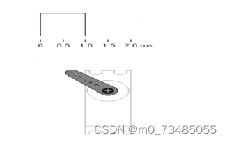
3.5.2 舵机SG90
(1)模块工作原理
控制信号由接收机的通道进入信号调制芯片,获得直流偏置电压。它内部有一个基准电路,产生周期为20ms,宽度为1.5ms的基准信号,将获得的直流偏置电压与电位器的电压比较,获得电压差输出。最后,电压差的正负输出到电机驱动芯片决定电机的正反转。当电机转速一定时,通过级联减速齿轮带动电位器旋转,使得电压差为0,电机停止转动。
(2)管脚介绍
红 - 舵机电源脚,接5V电源即可
棕 –舵机GND
橙 - 数据控制线
(3)舵机的控制
SG90 脉冲周期为20毫秒(millisecond) 也就是说最多1秒钟内可以转动50次,但是考虑到每次转动还要耗时,所以实际达不到50次。PWM控制信号周期20ms,脉宽0.5ms-2.5ms对应的角度-90到+90度,范围180度(3度左右偏差),当脉宽1.5ms时舵机在中立点(0度),我们直接用Python的GPIO提供的PWM控制。脉宽0.5ms-2.5ms 对应的占空比为2.5% - 12.5% . 理论上,10%的空间可以提供180度的线性分割。
以180度角度伺服为例,那么对应的控制关系是这样的:
0.5ms--------------0度;
1.0ms------------45度;
1.5ms------------90度;
2.0ms-----------135度;
2.5ms-----------180度;
舵机原理
四、 软件设计
4.1环境准备
4.1.1 环境安装
1.电脑与树莓派命令行连接
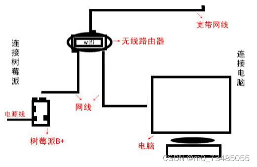
树莓派电脑连接图
1.树莓派网线连接路由器,电脑也连接在该路由器下即在同一局域网内
2.进入路由器管理界面,在DHCP服务内获取树莓派ip
3.在电脑上利用X-shell软件通过ssh远程访问路由器
X-shell界面显示如下
Connecting to 192.168.1.104:22…
Connection established.
To escape to local shell, press Ctrl+Alt+].
The programs included with the Debian GNU/Linux system are free software;
the exact distribution terms for each program are described in the
individual files in /usr/share/doc/*/copyright.
Debian GNU/Linux comes with ABSOLUTELY NO WARRANTY, to the extent
permitted by applicable law.
Last login: Thu May 11 19:25:38 2017
SSH is enabled and the default password for the ‘pi’ user has not been changed.
This is a security risk - please login as the ‘pi’ user and type ‘passwd’ to set a new password.
pi@raspberrypi:~ $
2.电脑与树莓派图形化界面连接
1.在系统内安装VNC
sudo apt-get install tightvncserver
2.配置vnc
sudo nano /etc/init.d/tightvncserve
修改如下:
#!/bin/sh
su $USER -c ‘/usr/bin/tightvncserver -kill :1’
echo “Tightvncserver stopped”
;;
*)
echo “Usage: /etc/init.d/tightvncserver {start|stop}”
exit 1
;;
esac
exit 0
3.然后使用 ctrl+X 的组合键退出,选择 Y 回车确认继续给 tightvncserver 文件加执行 权限,继续输入下面
sudo chmod 755 /etc/init.d/tightvncserver
继续输入下面命令 sudo update-rc.d tightvncserver defaults
最后输入执行命令: vncserver
在Windows上执行VNC-Viewer-6.1.0-Windows-64bit.exe输入IP密码即可进入系统桌面
4.电脑与树莓派文件传输
在Windows上安装FileZilla Client软件利用获知的IP利用SFTP协议登陆
5.手机与树莓派蓝牙连接
A)安装蓝牙协议Bluez
1)首先更新系统,并安装必备的软件库
sudo apt-get update
sudo apt-get upgrade
sudo apt-get install libdbus-1-dev libdbus-glib-1-dev libglib2.0-dev libical-dev libreadline-dev libudev-dev libusb-dev make wget
2)然后下载Bluez最新源码:
wget https://www.kernel.org/pub/linux/bluetooth/bluez-5.37.tar.xz
tar xvf bluez-5.37.tar.xz
cd bluez-5.32
3)然后进行编译,编译比较耗费时间:
./configure --disable-systemd
Make
4)编译完成后,进行安装,此时需要安装至系统目录下,所以需要sudo命令:
sudo make install
B)安装bluepy
安装完成后,我们可以使用hcitool的命令行工具集来调试我们的蓝牙设备,但是为了封装更多的逻辑那么我们就要使用编程语言来调用Bluez协议栈,此处使用开源社区qithub开发的工具包,bluepy
#克隆代码库,进行编译
git clone https://github.com/IanHarvey/bluepy.git
#根据文档可知,该库只支持bluez-5.3及以上版本,我们安装的是5.37所以可以直接make
cd bluepy/bluepy
make
C)修改配置
让蓝牙以兼容模式启动
sudo nano /etc/systemd/system/dbus-org.bluez.service
修改内容如下:
ExecStart=/usr/lib/bluetooth/bluetoothd -C
ExecStartPost=/usr/bin/sdptool add SP
4.1.2 开发语言(GPIO编程)
(1)python GPIO
【开发语言】——python
【简单介绍】——该库更确切的名称为raspberry-gpio-python,树莓派官方资料中推荐且容易上手。python GPIO是一个小型的python库,可以帮助用户完成raspberry相关IO口操作。但是python GPIO库还没有支持SPI、I2C或者1-wire等总线接口。除了python GPIO之外,还有众多的python扩展库(例如webiopi),毫无疑问的说python非常适合树莓派,树莓派也非常适合python。
【1】先安装python-dev,输入以下指令。
sudo apt-get install python-dev
【2】安装RPi.GPIO,依次输入以下指令。特别说明,由于RPi.GPIO仍处于不断完善的过程中,请参考前言中的链接下载最新的安装代码。
下载
$ wget http://raspberry-gpio-python.googlecode.com/files/RPi.GPIO-0.5.3a.tar.gz
解压缩
$ tar xvzf RPi.GPIO-0.5.3a.tar.gz
进入解压之后的目录
$ cd RPi.GPIO-0.5.3a
启动安装
$ sudo python setup.py install
(2)wiringPi
【开发语言】——C语言
【简单介绍】——wiringPi适合那些具有C语言基础,在接触树莓派之前已经接触过单片机或者嵌入式开发的人群。wiringPi的API函数和arduino非常相似,这也使得它广受欢迎。作者给出了大量的说明和示例代码,这些示例代码也包括UART设备,I2C设备和SPI设备等,毫无疑问地说wiringPi功能非常强大。
1)方案A——使用GIT工具
通过GIT获得wiringPi的源代码
git clone git://git.drogon.net/wiringPi
cd wiringPi
./build
build脚本会帮助你编译和安装wiringPi
2)方案B——直接下载
我们可以在https://git.drogon.net/?p=wiringPi;a=summary网站上直接下载最新版本编译使用
tar xfz wiringPi-xx.tar.gz
cd wiringPi-xx
./build
3、测试:
wiringPi包括一套gpio命令,使用gpio命令可以控制树莓派上的各种接口,通过以下指令可以测试wiringPi是否安装成功。
$gpio -v
$gpio readall
(3)BCM2835 C Library
【开发语言】——C语言
【简单介绍】BCM2835 C Library可以理解为使用C语言实现的相关底层驱动,它给我的感觉更像STM32的库函数,BCM2835 C Library的驱动库包括GPIO、SPI和UART等,可以通过学习BCM2835 C Library熟悉BCM2835相关的寄存器操作。如果有机会开发树莓派上的linux驱动,或自主开发python或PHP扩展驱动,可以从BCM2835 C Library找到不少的“灵感”。
下载
$ wget http://www.airspayce.com/mikem/bcm2835/bcm2835-1.35.tar.gz
解压缩
$ tar xvzf bcm2835-1.35.tar.gz
进入压缩之后的目录
$ cd bcm2835-1.35
配置
./configure
从源代码生成安装包
make
执行检查
sudo make check
安装 bcm2835库
sudo make install
下图为三种方式对应引脚图
引脚图
(4)语言选择
1.python入门较为简单。
2.python语言适用范围较广,前景较好。
3.树莓派支持官方原生语言为python。
4.1.3软件安装
(1)redis
由于模块之间需要消息传递需要安装redis。
redis是一个key-value存储系统。和Memcached类似,它支持存储的value类型相对更多,包括string(字符串)、list(链表)、set(集合)、zset(sorted set --有序集合)和hash(哈希类型)。这些数据类型都支持push/pop、add/remove及取交集并集和差集及更丰富的操作,而且这些操作都是原子性的。在此基础上,redis支持各种不同方式的排序。与memcached一样,为了保证效率,数据都是缓存在内存中。区别的是redis会周期性的把更新的数据写入磁盘或者把修改操作写入追加的记录文件,并且在此基础上实现了master-slave(主从)同步。
安装软件
wget http://download.redis.io/releases/redis-3.0.6.tar.gz
tar xzf redis-3.0.6.tar.gz
cd redis-3.0.6
make
启动软件
redis-server
启动客户端
redis-cli
(2)Python操作Redis
安装
sudo pip install redis
or
sudo easy_install redis
or
源码安装
详见:https://github.com/WoLpH/redis-py
操作模式
redis-py提供两个类Redis和StrictRedis用于实现Redis的命令,StrictRedis用于实现大部分官方的命令,并使用官方的语法和命令,Redis是StrictRedis的子类,用于向后兼容旧版本的redis-py。
#!/usr/bin/env python
-- coding:utf-8 --
import redis
r = redis.Redis(host=‘10.211.55.4’, port=6379)
r.set(‘foo’, ‘Bar’)
print r.get(‘foo’)
连接池:
redis-py使用connection pool来管理对一个redis server的所有连接,避免每次建立、释放连接的开销。默认,每个Redis实例都会维护一个自己的连接池。可以直接建立一个连接池,然后作为参数Redis,这样就可以实现多个Redis实例共享一个连接池。
#!/usr/bin/env python
-- coding:utf-8 --
import redis
pool = redis.ConnectionPool(host=‘10.211.55.4’, port=6379)
r = redis.Redis(connection_pool=pool)
r.set(‘foo’, ‘Bar’)
print r.get(‘foo’)
操作
String操作,redis中的String在在内存中按照一个name对应一个value来存储。如下所示:
Name value
N1 --------- v1
N2 --------- v2
N3 --------- v3
4.2程序设计
4.2.1 信息采集子程序设计
Fun_se.py
该程序的作用是驱动舵机并且定义接口def turn(s,t)在模块Mode_auto_us中配合超声波进行侦测避障。
关键代码见程序清单1
Fun_us.py
该程序的作用是驱动超声波对前方障碍物进行探测并计算距离,并且定义接口def shot(op,ip) 在模块Mode_auto_us中配合舵机进行侦测避障。
关键代码见程序清单2
Fun-speed.py
该程序的作用是驱动槽型光电传感器对车轮速度进行检测并上传数据到redis。
关键代码见程序清单3
4.2.2 信息处理分析子程序设计(主程序)
Mode_auto_us.py
该程序的作用是:
1.收集来自蓝牙模块传到redis的数据,通过while对指令判断执行等待、退出、运行超声波舵机结合避障。
2.收集来自Fun_se.py和 Fun_us.py的距离数据和舵机数据。
3.依据收集的执行指令和来自Fun_se.py和 Fun_us.py的数据结合判断小车的执行情况。
4.依据执行情况调用Run_auto_moto.py的接口。
5.将执行结果情况沿redis传递至蓝牙模块Com_bluetooth.py中。
关键代码见程序清单4
Mode_auto_ir.py
该程序的作用:
1.收集来自YL-70传感器的数据。
2.收集来自蓝牙模块传到redis的数据,通过while对指令判断执行等待、退出、运行红外避障。
3.依据收集的执行指令和来自YL-70传感器的数据结合判断小车的执行情况。
4. 将执行结果情况沿redis传递至蓝牙模块Com_bluetooth.py中。
程序的关键代码见程序清单5
4.2.3 运动控制子程序设计
Run_auto_moto.py与Run_mt_moto.py
该模块提供对小车操纵即前后左右的接口方便蓝牙模块Com_bluetooth.py和红外避障模块Mode_auto_ir.py还有超声波舵机结合避障模块Mode_auto_us.py的调用。
程序的关键代码见程序清单6
4.2.4 工作状态子程序技术
利用redis的get与set函数和连接池对工作状态进行判断
在Com_bluetooth.py中定义在Mode_auto_us.py和Mode_auto_ir.py中连接
程序的关键代码见程序清单7
4.2.5 通讯程序技术(主程序)
本设计采用蓝牙串口通讯,且pybluez的库,提供了基于套接字的蓝牙串口通信接口。
首先进行架构的设计。考虑到树莓派需要同时连接多个手机,接收多个手机发来的消息,并作出相应,所以应当将树莓派作为套接字的服务端,手机作为客户端。
socket在服务器端的工作原理。作为一个服务器,需要监听端口,等待客户端的连接。当有客户端连接时,新开一个线程专门服务新链接,用于处理新连接的所有请求数据。
在pybluez中提供了一个BluetoothSocket类,用于生成socket对象。在BluetoothSocket类中拥有与socket类类似的结构,所以使用方法也类似。
第一步是创建一个BluetoothSocket对象,使其运行在服务器模式下,等待其他设备的连接,通信协议选择RFCOMM:
随后,使用accept函数接受新的连接,这个函数的返回值是元组,其中包含了新连接的信息,这里我使用的RFCOMM协议返回的元组中第一个是一个连接对象,另一个是一个信息表。这里直接使用一个死循环来处理这些事情,无需担心死循环会过多占用资源,对于accept函数,如果没有新链接,则会阻塞当前线程,也就不会占用CPU时间了。之后的就是开线程服务这个连接了。
程序的关键代码见程序清单8
五. 测试数据、测试结果分析及结论
硬件测试方法与仪器:
1、测试仪器
测试仪器包括秒数字万用表等。
2、测试方法
数字万用表主要用来测试分立元件的电阻、压降、漏电流、截止/导通状态等参数;
软件测试方法
1.将子模块分别加入main函数分别测试每个子模块实现情况
2.对与智能小车的前后左右实现分别编写程序测试
6. 致 谢
历时三个月的设计过程中,我首先边查资料,学习传感器知识,学习Python语言,学习GPIO编程,一边在基地对传感器进行测试。在编写过程中,我感觉到即使是一个简单的程序由于不断安装软件和配置环境都会导致成功实现的代码出各种各样的问题,要想很轻松的实现,也不是很容易的事情。
在安装Raspberry Pi的操作系统Raspdebain时按照网上流程顺利完成,但由于手旁没有可用的HDMI或者VGA线连接显示器,采用了ssh的方式电脑远程操作
在获取IP时出现各种问题后改用路由器成功登陆到系统内,开始按照流程对系统更新和配置。
在安卓手机与树莓派连接时,由于树莓派蓝牙未开发完全只能手动安装bluez蓝牙协议,并使用bluepy封装的蓝牙套接字对蓝牙串口进行操纵。在这过程中安装bluez产生了各种各样的报错,且蓝牙无法正常使用,经百度后将蓝牙改为兼容模式启动,经此成功实现手机与树莓派蓝牙通讯。
在实现对蓝牙信息处理时先采用了while True循环但问题百出,后将各模块独立而不是一个整体并使用redis消息队列使多个模块互相通讯,成功实现对来自蓝牙端的命令识别判断并回传结果。
在使用python语言中,由于书写格式的不严谨导致多次模块连接失败,这使我深深感受到理论与实际间的差距。
在设计蓝牙通讯时sockserver的编程和多线程处理的应用使我的编程能力大大提高。
在对硬件的接线中由于接线的不正确导致模块烧毁
通过这样的设计,提高了我的动手能力。每天上机编程,使我软件调试知识也提高了。
本设计采用的是树莓派3,这主要是因为该机的稳定性比较好可以简化编程
本设计在接近三个月的时间后接近尾声,作为一名大四的本科生,由于专业知识的不完整、不系统性和开发经验的匮乏,尤其是自学硬件知识和Python语言,设计和编写难免有考虑不到的地方,在这里衷心感谢毕业设计的校内指导老师和杰普软件基地的指导老师的督促和指导,感谢本科校内老师传授的专业知识和帮助。感谢同窗好友的鼓励和支持。感谢网络无私贡献知识的网友。如果没有以上人等的支持和帮助,那么我的毕业设计将完成的很艰辛,他们在设计中给了我很多意见和建议。同时也要感谢自己在多次遇到困难的时候没有一蹶不振,取而代之的是不断查阅资料去寻求解决方案,使我找到了最好的方法来解决问题。最后,感谢生我养我的父母。谢谢他们给了我无私的爱,为我求学所付出的巨大牺牲和努力,在我遇到困难时鼓励我走出困境。
7. 参 考 文 献
[1] 黄智伟.全国大学生电子设计竞赛系统设计[M].北京:北京航空航天大学出版社,2007年2月。.
[2] 李瀚霖等.智能小车研究与设计[J]. 科技致富向导,2011年26期…
[3] 尹念东.智能车辆的研究及前景[J].上海汽车,2002.2.
[4] 赵振德. 多功能遥控智能小车的制作[J]. 电子制作, 2011年4期.
[5] 陈铁军. 智能控制理论及应用[M]. 北京:清华大学出版社,2009.1.
[6] 刘南平. 电子产品设计与制作技术[J]. 科学出版社,2008.
[7] 于连国,李伟,王妍玮. 基于单片机的智能小车设计[J]. 林业机械与木工设备, 2011年4期.
[8] Rowel O.Atienza,Marcelo H. Ang Jr. A Flexible Control Architecture for Mobile Robots: An Application for a Walking Robot[J]. Journal of Intelligent and Robotic Systems, Springer Netherlands, 2001,1(30), 29~48
[9] Zhu, W., Ruan, H. Design and research of solar photovoltaic power generation controller based on 89C51 microcontroller. Advanced Materials Research 345, 2011,pp. 66-69.
[10] J Borenstein,Y Koren.Obstacle avoidance with ultrasonic sensors,1998
附录A 程序清单
附录程序1
Fun_us.py
n=2
bj=400
k=0
for i in range(n):
gpio.output(op,1)
time.sleep(0.2)
gpio.output(op,0)
tt=0
while gpio.input(ip)==0:
tt+=1
continue
s=time.time()
tt=0
while gpio.input(ip)==1:
tt+=1
if tt>=bj : break
continue
t=time.time()
ds=(t-s)*34300/2
k+=ds
#print ds," ",tt
while gpio.input(ip)==1: continue
k=k//n
return k
附录程序2
Fun_se.py
def turn(s,t):
k=s
if s<=t:
while k<=t:
p.ChangeDutyCycle(2.5 + 10 * k / 180)
time.sleep(0.02)
p.ChangeDutyCycle(0)
time.sleep(0.02)
k+=10
while k>=t:
p.ChangeDutyCycle(2.5 + 10 * k / 180)
time.sleep(0.02)
p.ChangeDutyCycle(0)
time.sleep(0.02)
k-=10
附录程序3
N=1.02101761
count = 0
print “0”
try:
wd=r.get('status')

while wd=='q':

	into = GPIO.input(INTO)
	print "1"
	if into==0:
		print "2"
		count+=count
		if 1000==count:
			print '3'
			vel =N*(count/20);
			sp=vel+'cm/s(R)'
			r.set('speed',sp)
			count = 0
附录程序4
Mode_auto_us.py
地图程序
max=320
MP=[[0 for X in range(max)] for y in range(max)]
DIR=1
JD=13
XX=0; YY=0
class pin:#超声波IO
ip=36 #Echo
op=32 #Trig
class Auto:
@staticmethod
def Map(x,y):
global MP,DIR
global JD
if DIR==1:
  fx=x; fy=y-1
  lx=x-1; ly=y
  rx=x+1; ry=y
if DIR==2:
  fx=x+1; fy=y
  lx=x; ly=y-1
  rx=x; ry=y+1
if DIR==3:
  fx=x; fy=y+1
  lx=x+1; ly=y
  rx=x-1; ry=y
if DIR==4:
  fx=x-1; fy=y
  lx=x; ly=y+1
  rx=x; ry=y-1

s=Fun_us.shot(pin.op,pin.ip)
if s<JD: MP[fx][fy]=2
if MP[fx][fy]==0: return 2
else:
  Fun_se.turn(0,90)
  s=Fun_us.shot(pin.op,pin.ip)
  Fun_se.turn(90,180)
  if s<JD: MP[rx][ry]=2
  if MP[rx][ry]==0: return 1

  Fun_se.turn(180,90)
  s=Fun_us.shot(pin.op,pin.ip)
  Fun_se.turn(90,0)
  if s<JD: MP[lx][ly]=2
  if MP[lx][ly]==0: return 1
  if MP[fx][fy]==1: return 1
  if MP[rx][ry]==1: return 2
  if MP[lx][ly]==1: return 2
  return 1
@staticmethod
def cd(cds):
global DIR
if cds1: DIR+=1
if cds2: DIR-=1
if DIR>4: DIR=4
if DIR<1: DIR=1
return dir
@staticmethod
def mapout(kx):
for i in range(kx):
s=“”
for j in range(kx):
s+=str(MP[160-kx2+j][160-kx2+i])
print s
主程序
try:
while True:
wd =r.get('status')

if wd=='es':
  print "Now you exit the Auto_us MODE "
  r.set('print','exit')
  gpio.cleanup()
  sys.exit(0)
elif wd=='uo':
  print "Now Mode_auto_us is waitting "
  time.sleep(1)
  r.set('print','running')
elif wd=='us':
  print "Now the Auto_ir MODE is running"
  r.set('print','pause')

  global JD
  global MODE
  Run_auto_moto.Car.stop()

  x=max//2; y=max//2
  MP[x][y]=1
  d=Auto.Map(x,y)
  if d==1:
    #kx+=1
    Run_auto_moto.Car.back()
    if DIR==1: y-=1
    if DIR==2: x+=1
    if DIR==3: y+=1
    if DIR==4: x-=1
  elif d==2:
    Run_auto_moto.Car.right()
    Auto.cd(1)
  elif d==3:
    Run_auto_moto.Car.left()
    Auto.cd(2)
  MP[x][y]=1
  print "Run mode:",d,"  Direction:",DIR
  #Auto.mapout(10)
  time.sleep(0.2)
raw_input()
except Exception, e:
print “Sorry for the error, I have to suspend this service for you”
r.set(‘print’,‘wrong’)
gpio.cleanup()
附录程序5
Mode_auto_ir.py
try:
while True:
            wd =r.get('status')

            if wd == 'io' :

                    print "Now Mode_auto_ir is waitting "
                    time.sleep(1)
                    #GPIO.cleanup()
                    r.set('print','running')
                    #breakyou exit the Auto_ir MODE and

            elif wd == 'er':
                    print "Now you exit the Auto_ir MODE "
                    GPIO.cleanup()
                    sys.exit(0)

            elif wd == 'ir':

                    print "Now the Auto_ir MODE is running"
                    r.set('print','exit')

                    BLL = GPIO.input(LL)
                    BLR = GPIO.input(LR)
                    BRL = GPIO.input(RL)
                    BRR = GPIO.input(RR)

                    if BLL == True and BLR == True and BRL == True and BRR == True:
                            Run_auto_moto.Car.back()
                            print "1"
                    time.sleep(0.4)
    raw_input()
except Exception, e:
print “Sorry for the error, I have to suspend this service for you”
r.set(‘print’,‘wrong’)
GPIO.cleanup()
附录程序6
class wheel :
pins={‘lt’:[35,37],‘rt’:[33,31]}
def init(self,name):
self.name=name
self.pin=wheel.pins[self.name]
gpio.setmode(gpio.BOARD)
gpio.setup(self.pin[0],gpio.OUT)
gpio.setup(self.pin[1],gpio.OUT)
gpio.output(self.pin[0],0)
gpio.output(self.pin[1],0)
self.stop()
def fowd(self):
gpio.output(self.pin[0],gpio.HIGH)
gpio.output(self.pin[1],gpio.LOW)
def stop(self):
gpio.output(self.pin[0],False)
gpio.output(self.pin[1],False)
def back(self):
gpio.output(self.pin[0],gpio.LOW)
gpio.output(self.pin[1],gpio.HIGH)
class Car :
wheels=[wheel(‘lt’),wheel(‘rt’)]
@staticmethod
def init():
gpio.setmode(gpio.BOARD)
for wheel in Car.wheels: wheel.stop()
@staticmethod
def stop():
for wheel in Car.wheels: wheel.stop()
@staticmethod
def fowd():
Car.stop()
for wheel in Car.wheels: wheel.fowd()
time.sleep(0.5)
Car.stop()
@staticmethod
def back():
Car.stop()
for wheel in Car.wheels: wheel.back()
time.sleep(0.5)
Car.stop()
@staticmethod
def left():
Car.stop()
Car.wheels[1].fowd()
Car.wheels[0].back()
time.sleep(0.3)
Car.stop()
@staticmethod
def right():
Car.stop()
Car.wheels[0].fowd()
Car.wheels[1].back()
time.sleep(0.3)
Car.stop()
附录程序7
初始化
r=redis.Redis(host=‘127.0.0.1’,port=6379)
连接池
pool = redis.ConnectionPool(host=‘127.0.0.1’, port=6379)
r = redis.Redis(connection_pool=pool)
附录程序8
主线程
server_socket.bind((“”,1))
server_socket.listen(1);
while True:
sock,info=server_socket.accept();
print(str(info[0])+’ Connected!‘);
t=threading.Thread(target=serveSocket,args=(sock,info[0]))
t.setDaemon(True)
t.start();
套接字
def serveSocket(sock,info):
while True:
receive=sock.recv(1024).decode(‘utf-8’);
print(’[‘+str(info)+’]'+receive);
r.set(‘status’,receive)
pt=r.get(‘print’)+“\n”
sock.send(pt)
sock.send(‘speed’)
附录B 硬件原理图
A
B
图1 直流电机接线图(以上两图AB)
图2 槽型光电测速模块连接图
图3 红外模块连接图
图4 光电码盘测速图
外文翻译
英文原文
The Design of a Rapid Prototype Platform for ARM Based Embedded System
Hardware prototype is a vital step in the embedded system design. In this paper, we discuss our design of a fast prototyping platform for ARM based embedded systems, providing a low cost solution to meet the request of flexibility and testability in embedded system prototype development. It also encourages concurrent development of different parts of system hardware as well as module reusing.
Though the fast prototyping platform is designed for ARM based embedded system, our idea is general and can be applied to embedded system of other types. I.INTRODUCTION
Embedded systems are found everywhere, including in cellular telephones, pagers, VCRs, camcorders, thermostats, curbside rental-car check-in devices, automated supermarket stockers, computerized inventory control devices, digital thermometers, telephone answering machines, printers, portable video games, TV set-top boxes – the list goes on. Demand for embedded system is large, and is growing rapidly.
In order to deliver correct-the-first time products with complex system requirements and time-to-market pressure, design verification is vital in the embedded system design process. A possible choice for verification is to simulate the system being designed. If a high-level model for the system is used, simulation is fast but may not be accurate enough, with a low-level model too much time may be required to achieve the desired level of confidence in the quality of the evaluation. Since debugging of real systems has to take into account the behavior of the target system as well as its environment, runtime information is extremely important. Therefore, static analysis with simulation methods is too slow and not sufficient. And simulation cannot reveal deep issues in real physical system.
A hardware prototype is a faithful representation of the final design, guarantying its real-time behavior. And it is also the basic tool to find deep bugs in the hardware. For these reasons, it has become a crucial step in the whole design flow. Traditionally, a prototype is designed similarly to the target system with all the connections fixed on the PCB (printed circuit boards).
As embedded systems are getting more complex, the needs for thorough testing become increasingly important. Advances in surface-mount packaging and multiple-layer PCB fabrication have resulted in smaller boards and more compact layout, making traditional test methods, e.g., external test probes and “bed-of-nails” test fixtures, harder to implement. As a result, acquiring signals on boards, which is beneficial to hardware testing and software development, becomes infeasible, and tracking bugs in prototype becomes increasingly difficult. Thus the prototype design has to take account of testability. However, simply adding some test points is not enough. If errors on the prototype are detected, such as misconnections of signals, it could be impossible to correct them on the multiple-layer PCB board with all the components mounted. All these would lead to another round of prototype fabrication, making development time extend and cost increase.
Besides testability, it is important to maintain high flexibility during development of the prototype as design specification changes are common. Nowadays complex systems are often not built from scratch but are assembled by reusing previously designed modules or off-the-shelf components such as processors, memories or peripheral circuitry in order to cope with more aggressive time-to-market constraints. Following the top-down design methodology, lots of effort in the design process is spent on decomposing the customers, requirements into proper functional modules and interfacing them to compose the target system.
Some previous research works have suggested that FPLDs (field programmable logic device) could be added to the final design to provide flexibility as FPLDs can offer programmable interconnections among their pins and many more advantages. However, extra devices may increase production cost and power dissipation, weakening the market competition power of the target system. To address these problems, there are also suggestions that FPLDs could be used in hardware prototype as an intermediate approach [1]-[3], whereas this would still bring much additional work to the prototype design. Moreover, modules on the prototype cannot be reused directly. In industry, there have been companies that provide commercial solutions based on FPLDs for rapid prototyping [4]. Their products are aimed at SOC (system on a chip) functional verification instead of embedded system design and development.
In this paper, we discuss our design of a Rapid Prototyping Platform for ARM based Embedded System, providing a low cost solution to meet the request of flexibility and testability in embedded system prototype development. It also encourages concurrent development of different parts of system hardware as well as module reusing. The rest of the paper is organized as follows. In section 2, we discuss the details of our rapid prototyping platform. Section 3 shows the experimental results, followed by an overall conclusion in section 4.
II. THE DESIGN OF A RAPID PROTOTYPING PLATFORM A. Overview
ARM based embedded processors are wildly used in embedded systems due to their low-cost, low-power consumption and high performance. An ARM based embedded processor is a highly integrated SOC including an ARM core with a variety of different system peripherals[5]. Many arm based embedded processors, e.g.[6]-[8], adopt a similar architecture as the one shown in Fig. 1.
The integrated memory controller provides an external memory bus interface supporting various memory chips and various operation modes (synchronous, asynchronous, burst modes). It is also possible to connect bus-extended peripheral chips to the memory bus. The on-chip peripherals may include interrupt controller, OS timer, UART, I2C, PWM, AC97, and etc. Some of these peripherals signals are multiplexed with general-purpose digital I/O pins to provide flexibility to user while other on-chip peripherals, e.g. USB host/client, may have dedicated peripheral signal pins. By connecting or extending these pins, user may use these onchip peripherals. When the on-chip peripherals cannot fulfill the requirement of the target system, extra peripheral chips have to be extended.
The architecture of an ARM based embedded system is shown in Fig. 2. The whole system is composed of embedded processor, memory devices, and peripheral devices. To enable rapid prototyping, the platform should be capable of quickly assembling parts of the system into a whole through flexible interconnection. Our basic idea is to insert a reconfigurable interconnection module composed by FPLD into the system to provide adjustable connections between signals, and to provide testability as well. To determine where to place this module, we first analyze the architecture of the system.
The embedded system shown in Fig. 2 can be divided into two parts. One is the minimal system composed of the embedded processor and memory devices. The other is made up of peripheral devices extended directly from onchip peripheral interfaces of the embedded processor, and specific peripheral chips and circuits extended by the bus.
The minimal system is the core of the embedded system, determining its processing capacity. The embedded processors are now routinely available at clock speeds of up to 400MHz, and will climb still further. The speed of the bus connecting the processor and the
memory chips is exceeding 100MHz. As pin-to-pin propagation delay of a FPLD is in the magnitude of a few nanoseconds, inserting such a device will greatly impair the system performance.
The peripherals enable the embedded system to communicate and interactive with the circumstance in the real world. In general, peripheral circuits are highly modularized and independent to each other, and there are hardly needs for flexible connections between them.
Here we apply a reconfigurable interconnection module to substitute the connections between microcomputer and the peripherals, which enables flexible adjusting of connections to facilitate interfacing extended peripheral circuits and modules. As the speed of the data communication between the peripherals and the processor is much slower than that in the minimal system, the FPLD solution is feasible.
Following this idea, we design the Rapid Prototyping Platform as shown in Fig. 3. We define the interface ICB between the platform and the embedded processor core boar that holds the minimal system of the target embedded system. The interface IPB between the platform and peripheral boards that hold extended peripheral circuits and modules is also defined. These enable us to develop different parts of the target embedded system concurrently and to compose them into a prototype rapidly, and encourage module reusing as well. The two interfaces are connected by a reconfigurable interconnect module. There are also some commonly used peripheral modules, e.g. RS232 transceiver module, bus extended Ethernet module, AC97 codec, PCMCIA/CompactFlash Card slot, and etc, on the platform which can be interfaced through the reconfigurable interconnect module to expedite the embedded system development. B. Reconfigurable Interconnect Module
With the facility of state-of arts FPLDs, we design a reconfigure interconnection module to interconnect, monitor and test the bus and I/O signals between the minimal system and peripherals.
As the bus accessing obeys specific protocol and has control signals to identify the data direction, the interconnection of the bus can be easily realized by designing a corresponding bus transceiver into the FPLD, whereas the interconnection of the I/Os is more complex. As I/Os are multiplexed with on-chip peripherals signals, there may be I/Os with bi-direction signals, e.g. the signals for on-chip I2C[9] interface, or signals for on-chip MMC (Multi Media Card[10]) interface. The data direction on these pins may alter without an external indication, making it difficult to connect them via a FPLD. One possible solution is to design a complex state machine according to corresponding accessing protocol to control the data transfer direction. In our design we assign specific locations on the ICB and IPB interfaces to these bi-direction signals and use some jumpers to directly connect these signals when needed. The problem is circumvented at the expense of losing some flexibility.
The use of FPLD to build the interconnection module not only offers low cost and simple architecture for fast prototyping, but also provides many more advantages. First, interconnections can be changed dynamically through internal logic modification and pin re-assignment to the FPLD. Second, as FPLD is connected with most pins from the embedded processor, it is feasible to detect interconnection problems due to design or physical fabricate fault in the minimal system with BST (Boundary-Scan Test, IEEE Standard 1149.1 specification). Third, it is possible to route the FPLD internal signals and data to the FPLD’s I/O pins for quick and easy access without affecting the whole system design and performance. It is even possible to implement an embedded logical analyzer into the FPLD to smooth the progress of the hardware verification and software development. C. Power Supply
Power dissipation has a great impact on system cost and reliability. It is an increasingly important problem in embedded systems designs not only for the portable electronics industry but in other areas including consumer electronics, industry control, communications, etc. In order to facilitate the design of power supply for the target embedded system, power supply issues have also been considered in the design of the platform.
First, the power supplies to the devices on the platform are separated from those to the core board and peripheral expand boards, which makes it more realistic to measure and verify the power dissipation on the platform for the target embedded system. Second, the power supplies for the core board and peripheral expand boards are built on a separate board and connected to the platform through a slot. As a result, it provides flexibility for power system design while speeding up the whole design process.
To meet the demand for higher system speed and lower power consumption in data communications and processing, embedded processor vendors use increasingly advanced processing technologies requiring lower core operating voltages, and keep the interface voltage compatible with most low voltage semiconductor devices on market. Consequently, almost every embedded processor requires more than one power supply, such as power supply for internal logic, for PLLs and oscillators, for memory bus interface, and for other I/Os. Further, different embedded processors may have different requirements on power supply, such as different power supply voltage, powerup sequence, and different strategies to adjust the core voltage in different CPU run mode for minimizing power dissipation.
A survey of some widely used ARM based embedded processor suggests that most of them need no more than 3 groups of separated power supply, as shown in Table 1. As the peripherals may require different supply voltages for special purpose, such as +5V for powering the USB ports, we divide the power supply from the power supply slot into 4 separated channels, which is connected to both the core board slot and the peripheral board slot. Each channel of power supplies has a “power good” signal to indicate power output status of the channel, and a shutdown signal to shut the power supply of the channel down. And these signals are directly connected to the core board slot to accommodate the embedded processor’s requirement of power-up sequence. In order to enable dynamic voltage adjusting, some control signals are routed to the power supply board by the reconfigurable interconnect module. III. EXPERIMENTAL RESULTS
As the Rapid Prototyping Platform is still under development, we present an example applied with the same considerations in the Rapid Prototyping Platform. It is an embedded system prototype based on Intel XScale PXA255, which is an ARM based embedded processor. The diagram of the prototype is illustrated in Fig. 5(a). The photo is shown in Fig. 5(b), where a Bluetooth module is connected to the prototype USB port and a CF LAN card is inserted.
The FPGA (an Altera Cyclone EP1C6F256) here offers the same function as the reconfigurable interconnection module shown in Fig. 3. Most of the peripheral devices are expanded to the system through the FPGA, and more peripherals can be easily interfaced when needed. As both of the FPGA and PXA255 support the BST, we can detect faults, e.g. short-circuit and opencircuit faults, on the connections between the two devices by chaining their JTAG ports and performing BST. Here, we use an open source software package [11] to perform the BST.
The FPGA internal signals can be routed to the debugging LED matrix for easy access, which is helpful in some simple testing and debugging. We also insert an embedded logical analyzer, the SignalTap II embedded logic analyzer [12] provided in Altera’s Quartus II software, into the FPGA for handling more complicated situations. With the help of the logical analyzer, we are able to capture and monitor data passing through over a period of time, which expedites the debugging process for the prototype system. Fig. 6 shows the captured data communication between the embedded processor and the USB host module during the initialization process of the Philips ISP1161 USB host chip[13]. It can be seen clearly from the figure that the embedded processor writes the command code of 0027H to address 01H (the ISP1161’s host controller command port) to access the HcChipID register, and reads 6120H (the chip’s ID) from address 00H (the ISP1161’s host controller data port).
The power supply module of the prototype system is held on a separate board connected to the system via a socket. We designed two power supply modules for the prototype system (shown in Fig. 7). One is a large module providing fixed output composed with simple but lowefficiency linear regulator (the upside one in the Fig. 7), the other is a compact module, capable of dynamic voltage adjusting, made up of complex highefficiency switch regulator(the downside one in the Fig. 7). The former module is first used to accommodate the basic power supply requirements during hardware test and relative software development. During the process, the later is developed and refined, and replaced the former one finally. The separation of power supply module from prototype allows refinement of the power supply module without affecting development of other parts of the system.
In this paper, we discuss the design of a fast prototyping platform for ARM based embedded systems to accommodate the requirements of flexibility and testability in the prototyping phase of an embedded system development.
With the aid of the platform, modules of the target embedded system can be developed simultaneously, and previous modules can be applied to future designs. As a result, develop process is greatly accelerated.
Though the fast prototyping platform is designed for ARM based embedded system, our idea is general and can be applied to embedded system of other types
.
中文翻译
基于ARM的嵌入式系统的速成样机平台设计
在嵌入式系统的设计中,硬件模型的设计是非常重要的。在这篇论文中,我们将讨论一种我们自行设计的快速模型平台,这是基于ARM的嵌入式系统的。这是一种低成本的设计方法,并且符合在嵌入式系统模型发展上对于灵活性和易测试性的要求。我们提供的方法同样支持系统硬件模块各个部分的更新和重利用。
虽然快速模型平台是为基于ARM的嵌入式系统设计的,但是我们的方法是普遍适用的而且可以被广泛应用于其它各种类型的嵌入式系统。
1.介绍
嵌入式系统的应用非常广泛,例如在手机、寻呼机、录像机、可携式摄像机、自动调温器、路边租用汽车的登记设备、自动售货机、用计算机处理存货清单的控制设备、数字体温计、电话应答机、打印机、便携式视频游戏、机顶盒——还可列出很多。对于嵌入式系统的需求是巨大的,同样它的发展也是很快的。
为了生产出满足复杂系统要求而且适应市场的正确的、第一手产品,设计的确认工作在整个设计过程中是非常关键的。对于确认,一个可能的选择是模仿已经设计出的系统。但是如果系统要求一个高水平的模型,,那么模仿虽然快可就不可能非常准确,因为低水平的模型只能满足一般质量评估的要求。一旦实时系统的调试要考虑进去,目标系统、还有它的环境、及其运行信息就显得特别重要。因此,用模仿的方法来做的静态分析机会让人感觉效率太低。而且模仿不能揭示在实时物理系统方面更深层次的问题。
一个硬件样机是最终设计的可考代表,它保证了实时行为。同时它也是发现硬件深层次问题的基础工具。正是由于这些原因,硬件样机设计成为整个设计流程中非常重要的一步。传统上,样机设计的都与它的目标系统的PCB版很相似。
随着嵌入式系统变得越来越复杂,对于系统的测试就显得越来越重要。表面设置组件和多层PCB板的发展,导致了更小的板子和更紧凑的版面设计。这就使得传统的测试方法,例如:外部探测器和“钉板”测试装置,很难实现。结果,从板子上获得对硬件测试和软件开发有用的信号变得不可行,而且使在样机上查找错误变得越来越难。因此,样机的设计必须考虑可测试性。然而,简单的加一些测试点是不够的。如果样机上的错误被检测出来,比如信号的错误连接,那么那是不可能在多层且与各种设置都紧密相关的PCB板上纠正的。因为这些都会影响到样机上的其它设置,增加项目开发的时间同时会提高成本。
除了可测试性,保持样机在开发过程中的高度灵活性也是非常重要的,因为设计规格是会经常改动的。目前复杂系统常常不是拼凑在一起的,而是会利用先前已经设计的一些模块,像是:处理器、存储器、或是外围电路。这样做是为了应付越来越激烈的市场竞争的压力。按照这些严密的方法论,我们就会明白设计时的大部分精力放在:将用户的需求拆分成合适的功能模块和再组成目标系统上。
很多以前的研究结论建议:将FPLDs添加到最终的设计中以增加系统的灵活性,因为FPLDs可以在它们的管脚间提供可编程的连接而且还可以带来其他一些好处。然而,外加设备可能会增加产品的成本和电源的负担,减弱目标系统的市场竞争力。除了这些问题,还有一个建议的方法就是将FPLDs在硬件样机中最为中介手段,,然而这种方法将会给样机的设计带来额外的工作。而且样机上的模块不能被直接重复利用。在市场上,有一些公司提供基于FPLDs的速成样机的商业解决方案。这些产品旨在对片上系统的功能检查,而不是以嵌入式系统的设计和发展为目标。
在这篇论文里,我们将提供自行设计的基于ARM的嵌入式系统的速成样机平台,这是一种低成本的解决方案,并且符合在嵌入式系统样机发展方面对于灵活性和可测试性的要求。它同样支持系统硬件各个部分的更新和模块的再利用。
论文剩下部分的结构是这样的:第二部分,我们将讨论自行设计的速成样机平台的细节。第三部分,将展示实验的结果,接下来的第四部分是全面的结论。 2.速成样机平台设计 A 总揽
基于ARM的嵌入式处理器被广泛应用于嵌入式系统,这是由于它们的低成本,低功耗和高性能。基于ARM的嵌入式处理器是高度集成的片上系统,它包括一个ARM内核,和各种各样地外围设备。很多基于ARM的嵌入式处理器,比如:[6]~[8]采用一种简单的结构就像Fig.1 所示。
集成存储器控制器提供外部存储器总线接口,这种接口支持各种各样的存储器芯片和各种操作模式(同步,异步,突发模式)。而且可以将扩展总线的外围芯片连接到存储器总线上。片上外围设备应该包括中断控制器,操作系统时钟,UART(通用异步收发器),I2C(两线式串行总线),PWM(脉宽调制),AC97(一种声卡)等等。其中一些外围设备的信号是多元的,它们都有多功能的数字I/O管脚来为用户提供方便,而其它的一些片上外围设备,例如:USB主机/客户机,就会提供专用的外围设备信号管脚。通过连接或是扩展这些管脚,用户可以利用这些片上外围设备。当片上外围设备不能满足目标系统的要求时,就得扩展额外的外围设备芯片。
基于ARM的嵌入式系统结构如图2所示。整个系统由嵌入式处理器,存储器设备,外围设备组成。为了设计成速成样机,那么平台应该可由各个模块通过灵活的方式迅速组装成一个整体。我们的基本方法是插入一个可重新配置的互相连接的模块,,然后用FPLD组成系统,并且使信号间的连接可调整,同时使其具有可测试性。在决定如何设置这样的模块之前,我们首先应该分析系统的结构。
在图Fig.2中展示的嵌入式系统可以被分为两部分。一部分是由嵌入式处理器和存储器设备构成的小型系统。另一部分是由嵌入式处理器的片上外围接口扩展的外围设备和有总线扩展的外围芯片、电路组成。
最小限度的系统是嵌入式系统的核心,它决定了嵌入式系统的处理能力。嵌入式处理器的时钟频率可以达到400MHz,而且可以达到更高。总线连接处理器和存储器的速度可以达到100MHz以上。因为FPLD的管脚间传播延时的数量级在十亿分之一秒,所以插入这样一个设备将会消弱系统的性能。。
外围设备可以使嵌入式系统与外界环境相通信和交互。一般来说,外围电路是高度模块化和独立化的。所以在它们之间几乎不需要设置什么灵活的连接手段。
这里我们运用可重新配置的相互连接的模块来代替微型计算机和外围设备之间的连接,这种方法可以实现灵活的连接,使模块和外围电路的接口配置变得容易。由于外围设备和处理器间的数据交换速度比最小限度系统要慢很多,所以用FPLD的方法是可行的。
按照这种思路,我们设计的速成样机平台如图3所示。我们在平台和载有最小限度嵌入式目标系统的嵌入式处理器核心开发板之间定义接口ICB。在平台和载有扩展的外围电路和模块的外围设备板之间定义接口IPB。这样做可以使我们同时更新嵌入式目标系统的各个模块,而且可以使它们快速组成一个样机,而且这种方法支持模块的再利用。ICB和IPB接口通过可重新配置的连接模块连接在一起。在结构图里也用到了一些外围模块,比如:RS-232模块,网口扩展模块,AC97,存储器卡槽等等。整个平台都通过可重新配置的连接模块来开发嵌入式系统。
用FPLD这一艺术级的设备,我们设计了用于在最小限度系统和外围设备之间联接、管理、测试总线和I/O信号的可重新配置的连接模块。
当符合具体协议的存取总线在控制信号来确认数据的传输方向时,我们可以通过在FPLDs里设计一个总线通信收发器连载监测这一行为。然而I/O管脚的这种互相连接会很复杂。由于I/O管脚的功能是复合,所以这会有拥有双向信号方向的I/O管脚,例如:给片上I2C(两线是串行总线)接口提供的信号,和给片上MMC(多媒体控制器)接口提供的信号。这些管脚上的数据传输方向再不需要外部信号的情况下是可以改变的,这就使得通过FPLDs来连接非常困难。一个可能的解决方案是根据通信协议设计一个复杂状态机,用以控制数据的传输方向。我们的设计方案里,在ICB和IPB接口的特殊位置放置双向信号管脚,然后利用跳线直接连接需要的信号管脚。但有一个问题是会减弱平台的灵活性。
利用FPLD来建立互相联接的模块,不仅仅是要提供低成本和简单的结构,更重要的是会带来很多其它好处。首先,通过在FPLD进行内部逻辑修改和管脚的重定位,会使连接可以实现动态改变。其次,由于FPLD与嵌入式处理器的大部分管脚相连,
这就使得用BST(Boundary-Scan Test, IEEE Standard 1149.1 specification)监测物理结构设计时出现的连接错误变得可行。再次,在不影响整个系统设计和性能的基础上,可以向FPLD的I/O引脚上发送FPLD内部信号和数据。而且甚至可以在FPLD内设置嵌入式逻辑分析器,使硬件的测试和软件的开发变得容易。 C 电源供应
电源的耗散会极大的影响系统的成本和可靠性。这现在已经在嵌入式系统设计上成为一个越来越重要的问题,而不仅仅是在便携式电子工业领域,而且在其它包括消费电子产品领域,工业控制领域,通信领域也变得越来越突出。为了使嵌入式系统的电源设计变得容易,电源问题也被纳入到平台设计的考虑范围之内。
首先,平台上设备的电源供应是与核心板和外围设备扩展板是分离的,这使得测量、核查嵌入式目标板的电源耗散更加容易。其次,为核心板和外围设备扩展板提供的电源是在一块分离的板子上的设制的,然后通过一个插槽与目标板相连。这样就可以设计出灵活的电源系统以加快整个设计的过程。
为了满足在数据传输和处理上的高速度和低功耗的要求,嵌入式处理期的商家使用更加高级的处理技术,而这种技术要求更加低的核心运行电压;同时商家要保证接口电压与市场上销售的低电压半导体设备相兼容。因此,几乎每一种嵌入式处理器都提供不止一个电源,例如为内部逻辑提供的电源,为相同步电路和振荡器提供的电源,为存储器总线接口提供的和为I/O引脚提供的。更进一步的说,不同的嵌入式处理器对电源有着不同的要求,比如不同的电源电压,加电顺序。在不同的CPU里,我们调整核心电压的不同方法,这些方法的运行模式都会使电压的耗散达到最小。
一项对基于ARM的嵌入式处理器的广泛调查表明,大部分都不需要多于3 组的独立电源,如TABLE 1所示。
由于不同的外围设备为不同的设计目的需要不同的电压,例如USB需要5 V的电压,我们将一个与核心板和外围设备板槽相连的电源供应槽分为4个频道。每一个电源供应频道会有显示电源输出状态良好的信号,及有关闭电源信道的关闭信号。这些信号直接与核心板的插槽相连接,用以调节嵌入式处理器对于加电顺序的要求。为使电压能够动态调节,一些控制信号可以通过可重新配置的互相连接模块发送到电源供应板子上。 3.试验结果
由于速成样机平台仍在发展,我们展示的例子就是运用这些已有的例子来设计的。这是一个基于Intel XScale PXA255的嵌入式系统样机。图5(a)展示了样机的结构。图5(b)是它的成品照片,蓝牙与样机的USB端口相连,且插入了CF LAN卡。
这里FPGA的功能就如图3 中的可重新配置的互相连接模块的功能。大部分外围设备都可通过FPGA连接到系统,很多外围设备都可根据需要方便的进行接口。因为FPGA和PXA255都支持BST,我们就可以进行测试,例如:可以通过JTAG口和BST的方法来检查两设备连接上的短路和开路错误。这里我们用开放软件包[11]来实现BST。
FPGA的内部信号可以很容易的发送给用于调试的发光二极管矩阵,这对于一些简单的调试和测试是非常有用的。我们也在FPGA中插入由Altera 公司的Quartus II 软件提供的SignalTap II嵌入逻辑分析仪,来处理更加复杂的情况。在逻辑分析仪的帮助下,我们可以获取和管理在很长一段时间内的数据传输情况。这样可以缩短样机系统的调试过程。如图6所示,就是逻辑分析仪俘获的在初始化Philips ISP1161 USB[13]主机芯片时,嵌入式处理器和USB主机模块的数据通信情况。
可以从描绘的图上清楚地看到嵌入式处理器在向地址01H(ISP1161主机控制器的命令端口)写0027H来获得主机控制器芯片ID寄存器,从地址00H(ISP1161主机控制器数据端口)读取6120H(芯片的ID)。
样机系统的电源供应模块被设置在一块单独的板子上,并通过一个插座与系统相连。我们为样机系统设计了两个电源模块。
一个是大模块由简单而低功耗的线性调整仪组成为固定输出提供电源(如图7的上部);另一个是比较紧凑的模块,有复杂且高效的非线性调整仪构成,它具有调节动态电压的能力(如图7 的下部所示)。先前的模块用来在硬件测试和软件开发时提供基础的电源。在开发的过程中,第二种方法出现并最终代替了第一种方法。由于电源供应模块是与样机相分离的独立模块,所以就可在不影响系统其他部分更新的情况下,来发展电源供应模块。
在这种灵活的样机的帮助下,我们最终在大约一星期内,完成了硬件开发和包括引导程序、操作系统(Arm-Linux)移植和驱动程序开发等软件设计的工作。 4.结论
在这篇论文里,我们论述了一种基于ARM的嵌入式系统的速成样机平台设计方法。这种方法是嵌入式系统发展的过程中,符合对样机的灵活性和可测试性要求的。
在样机平台的帮助下,嵌入式目标系统的各个模块均可独立更新,而且先前的一些模块也可以被运用到下一代的设计中。这样就大大加快了开发的过程。
虽然速成样机平台是为基于ARM的嵌入式系统设计的,但是我们的方法是普遍适用的,它也可以用于其他类型的嵌入式系统。

瓜分20万奖金 获得内推名额 丰厚实物奖励 易参与易上手
更多推荐

 1
1 0
0- 0


 已为社区贡献6条内容

所有评论(0)