CMOS中的 latch-up 闩锁效应、添加tap解决latch-up、使用combained area绘制TAP TAP的作用 IC后端版图【VLSI】
本文详细阐述了闩锁效应latch-up问题、如何通过添加Tap来解决。详细讲述了如何通过combained area来绘制TAP
CMOS中的 latch-up 闩锁效应、添加tap解决latch-up、使用combained area绘制TAP TAP的作用 IC后端版图【VLSI】
一、latch-up、Tap
本文详细阐述了latch-up问题、如何通过添加Tap来解决。
1. CMOS基础认知:N-Well和P-Substrate在CMOS里的位置
如下图所示,在N-well里的是NMOS,下图左边是NMOS,N-well与 其他p-substrate 隔离分开。

以PMOS举例,在PMOS的N-well里,N-well和经过P-type Diffusion后的P-active(下图中的p+)形成了一个PN结。为了把这个PN结反向偏置形成二极管隔离区域,我们把N-Well连接到高电压的VDD上,同时把P-Substrate连接到低电压GND上。。

但在工作期间,电荷会在 N-well中积聚。这种电荷会改变 P 沟道器件的电位差,从而可能导通这个PN结被正向偏置(Forwad Bias)。如果上面提到的PN结被导通的话,会形成Latch-Up效应,从而损坏整个芯片。
2. latch-up issue
- Latch Up is the Formation of low impedance path from Supply(VDD) to Ground(VSS) due to back to back connected parasitic Bipolar Junction Transistors(BJTs).These BJTs form Silicon Controlled Rectifier(SCR) with positive feedback and short the power and ground rail.
- Latch up comes due high nwell and pwell resistance, Due which potential difference creates that can on the internal transistors.latch-up establish low resistance conducting path between VDD (Supply) and GND (ground), which causes heavy current flow from VDD to GND.
- latch-up establish low resistance conducting path between VDD (Supply) and GND (ground), which causes heavy current flow from VDD to GND.

Latch-up 三种解决方案Prevention
- Guard ring. (Decrease the resistance )
- tap cells. (Decrease the resistance)
- Isolation trench. ( avoid undesired current leakage/ current conductive path)
3. 添加tap cells解决latch-up问题
Silicon substrate and well themselves in fact are relatively highly doped material, but for a good (low-ohmic) contact to metal you want it even higher doped - that’s why these Si-Metal contact regions get additional high(+) implant doses.

To avoid latch-up, p-substrate-tap (tied to Gnd) and n-well-tap (tied to Vdd) are inserted as frequently as possible. This has the effect of shorting out Rwell and Rsub. 从而阻止避免VDD直接相连到 GND的大电流导通。
3. TAP的基础概念
Think of what a faucet(Water Tap) looks like, which injected higher doping to Silicon substrate and well, provide a low-ohmic contact with the metal.
- p-substrate-taps and n-well-taps is concernign on the doping level, proper doping level will lead to gain less than 1 and preveting the current to increase
- Tap cells provide extra dopping of nwell, which lower the resistance.

n-well tap & p-substrate tap的工艺规则
这里的tap,指的是一块区域不单只一个东西。指的是,在n-well表面的一块区域,更深地掺杂n+离子(n-diffusion,版图里叫n-substratendiff),然后通过metal金属接到vdd/gnd
形象的解释见后文版图画法
The N-type material in the well is fairly resistive, so to ensure good control of potential multiple taps are needed for each N-well spread throughout the area.

- Substrate must be tied to GND and n-well to VDD
- Metal to lightly-doped semiconductor forms poor
connection (parasitic diode) - Use heavily doped well and substrate contacts
In a similar way, P+ substrate taps are added to the P-type substrate to control charge build-up in the substrate.
排列的个数
The process design rule manual (DRM) will specify a maximum distance between taps to avoid latch-up, but taps need to be inserted far more frequently to ensure good operation of an analog circuit.
经验法则:每 5-10 个晶体管放一个tap。
二、画版图layout时的TAP
Physical only cells是那些在网表中没有,而在实际芯片中需要存在的一些单元,如电源地IO、给IO供电的IO以及一些衬底、阱接触单元等。这里的TAP就是一种Physical only cells。
只是物理设计,并不是逻辑器件,可以用combained area这种画法绘制版图layout。
1. Magic
magic里:
n-well tap
- nwt是n-well tap,也叫nsubstratencontact
如前文所述,要掺杂地更浓,添加比较高的掺杂,在n-well区再加n,然后盖上metal1.
ps,虽然说,只是为了掺杂的更浓。我个人的理解,在用Magic软件画版图的时候需要把tap区域标清楚,就是需要有实心有对角线的nwt或pst,

 图1 在上面未盖metal1 图1 在上面未盖metal1
|
 图2 盖了metal1 图2 盖了metal1
|
p-substrate tap
- pst 是p-substrate tap也叫psubstratencontact
如前文所述,要掺杂地更浓,在p-sub区再加p,然后盖上metal1.

 图1 在上面未盖metal1 图1 在上面未盖metal1
|
 图2 盖了metal1 图2 盖了metal1
|
combained area 分层画法的解释:combined contact and tap
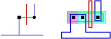
如上所展示,光在GND/VDD的电源轨道上“点”一个tap也可以,但是有的要求会要求画全。只能用于棒状图中diffusion末端与电源或接地轨的触点重合的情况(变成实心矩形)。注意这里,红色是polyscilion,蓝色是metal1,绿色是n-diffusion,粉红色是p-substrate,推断出是个NMOS。

We can often save space by using a combined contact and tap. Here the tap shares the same Active Area as the contact. A combined contact and tap is defined using a filled black square in place of the source contact (filled black circle).
A combined contact and tap can only be used where the end of a diffusion stick coincides with a contact to the power or ground rail.
引用:
https://secure.ecs.soton.ac.uk/notes/bim/notes/cad/guides/sticks.html
2.L-edit
==本例子是在P阱工艺下,即基底是N型的substrate衬底。==注意看这里没有n-well

n-substrate tap
在n-implement上增设active-area,然后加上TAP。如前文所述,要掺杂地更浓,在n-sub区再加n-imple,然后盖上metal1.

p-well tap
由于基底是n型材料,所以需要在底部加P-well。在p-implement上增设active-area,然后加上TAP。如前文所述,要掺杂地更浓,在p-well区再加p-imple,然后盖上metal1.

3. 画完tap后的自检
The following (process independent) guidelines should be considered when deciding on a cell layout.
- For simple functionality we require only one tap per N well and a single tap forthe whole wafer substrate
- Every well must have an appropriate tap.
- Every tap must be connected to a supply pad via unbroken metal.
- Taps should be placed as close to source connections as possible.
- Empirical rule: one tap for every 5-10 transistors.
- Layout N devices packed towards Vss and P devices packed towards Vdd.
三、Reference

开放原子开发者工作坊旨在鼓励更多人参与开源活动,与志同道合的开发者们相互交流开发经验、分享开发心得、获取前沿技术趋势。工作坊有多种形式的开发者活动,如meetup、训练营等,主打技术交流,干货满满,真诚地邀请各位开发者共同参与!
更多推荐
 已为社区贡献5条内容


所有评论(0)